
Understanding Laser Engraver PCBs
Overview of PCB Manufacturing
Understanding laser engraver PCB technology requires a deeper look into the intricate world of PCB manufacturing. Unlike traditional methods, laser engraving offers precision and speed that revolutionize how circuits are created. In South Africa, this innovation is gaining traction among small-scale manufacturers and hobbyists alike, driven by the desire for high-quality results without the hefty cost.
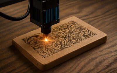
A laser engraver PCB process involves using focused laser beams to etch or cut the copper layers of a printed circuit board. This method not only speeds up production but also reduces waste, making it an attractive choice for custom designs and rapid prototyping. The accuracy of laser technology allows for complex geometries that would be difficult or impossible with conventional etching techniques.
For those venturing into laser engraver PCB creation, understanding the manufacturing flow is essential:
- Designing a detailed circuit layout using specialized software.
- Transferring the design onto the PCB substrate with precision laser engraving.
- Removing unwanted copper to reveal the final circuit pattern.
This streamlined process highlights the importance of choosing the right equipment and materials. As laser engraver PCB technology becomes more accessible, it’s transforming the landscape of electronics manufacturing in South Africa and beyond, making innovation more attainable for everyone.
What is Laser Engraving Technology?
Laser engraver PCB technology is transforming how we approach circuit board creation. At its core, laser engraving uses highly focused beams of light to precisely remove copper from a PCB substrate, carving out intricate circuit patterns with minimal waste. This method is not only faster than traditional etching but also offers a level of detail that was previously unimaginable.
Understanding laser engraver PCB involves grasping the core process: a laser beam targets specific areas, vaporizing or ablating the copper layer to reveal the desired circuit design. Unlike chemical etching, this technique is cleaner, environmentally friendly, and capable of producing complex geometries that challenge conventional methods. It’s this precision that makes laser engraver PCB a preferred choice among South African hobbyists and small-scale manufacturers seeking high-quality results.
- Accurate pattern transfer
- Reduced material waste
- Ability to create detailed and complex designs
As laser engraver PCB technology advances, its accessibility continues to grow, empowering more innovators to turn their ideas into tangible electronic prototypes quickly and efficiently. This shift is reshaping the landscape of electronics manufacturing in South Africa, making high-tech fabrication more inclusive than ever before.
Differences Between Laser Engraving and Traditional PCB Etching
When contrasting laser engraver PCB technology with traditional PCB etching, the differences aren’t just technical—they’re transformative. Traditional etching relies on chemical baths to dissolve unwanted copper, a process that often leaves behind hazardous waste and demands meticulous handling. In stark contrast, laser engraver PCB methods utilize concentrated beams of light to vaporize copper with pinpoint accuracy, significantly reducing chemical use and environmental impact.
This precision allows for the creation of intricate and complex designs that are nearly impossible to achieve through conventional means. For instance, laser engraver PCB can produce ultra-fine traces and detailed patterns without compromising the integrity of the substrate. Moreover, the speed of laser engraving drastically shortens production times, making it a game-changer for South African hobbyists and small-scale manufacturers eager to innovate swiftly.
To better understand the distinctions, consider these advantages of laser engraver PCB over traditional methods:
- Cleaner process—no chemicals or hazardous waste
- Superior detail and complex geometries achievable
- Reduced material waste, promoting sustainability
- Faster turnaround for prototypes and small batches
The evolution of laser engraver PCB technology continues to challenge old paradigms, offering a more precise, eco-friendly, and efficient pathway for circuit board fabrication. This shift not only elevates quality but also democratizes high-tech manufacturing across South Africa, opening new doors for innovation and creativity.
Advantages of Using Laser Engravers for PCB Production
High Precision and Detail
When it comes to producing high-quality printed circuit boards (PCBs), laser engraver pcb technology has revolutionized the industry with its unmatched precision. Unlike traditional methods, laser engraving allows for intricate detailing that is difficult to achieve manually or through chemical etching. This means that complex circuit designs can be created with minimal margin for error, ensuring every component aligns perfectly for optimal performance.
One of the key advantages of using a laser engraver pcb is the ability to achieve ultra-fine lines and tiny features, which are essential in modern electronics. The precision offered by laser technology ensures that even the smallest traces and pads are accurately etched, reducing the risk of defects that can compromise the entire circuit. This level of detail is particularly valuable in high-density PCB designs, where space is limited and accuracy is paramount.
Additionally, laser engravers enhance productivity and consistency. With automated control systems, once a design is uploaded, the process is swift and repeatable, making it ideal for both prototyping and mass production. The ability to quickly switch between different designs also means faster turnaround times, which is vital for staying competitive in today’s fast-paced tech landscape.
- High precision and fine detail
- Reduced risk of manufacturing defects
- Faster production cycles
- Enhanced design flexibility
Speed and Efficiency
In the fast-paced world of electronic manufacturing, speed and efficiency aren’t just luxuries—they’re survival skills. Enter the laser engraver PCB, a technological marvel that transforms the once laborious process into a streamlined symphony of precision and rapidity. Unlike traditional methods that involve lengthy chemical baths or painstaking manual work, laser engraving slashes production times dramatically. This means getting your prototype from concept to reality faster than ever before—crucial in a market where innovation waits for no one.
What truly sets a laser engraver PCB apart is its ability to handle multiple designs swiftly. With automated controls, switching from one intricate pattern to another is as simple as pressing a button. No more downtime or tedious setups. The result? Quicker turnaround times and a significant boost in productivity. Whether you’re producing small batches or mass manufacturing, laser engraving ensures each PCB is etched with consistent accuracy, reducing waste and defect rates.
In essence, a laser engraver PCB isn’t just about detailed artistry—it’s a powerhouse of speed and efficiency, making it an indispensable tool for forward-thinking electronics manufacturers. With the following advantages, it’s clear why more companies are embracing this cutting-edge technology:
- Accelerated production cycles
- Reduced manual intervention
- Rapid design iteration
- Minimal setup time
So, if staying ahead in the competitive electronics landscape sounds appealing, investing in laser engraver PCB technology might just be your smartest move yet. After all, when it comes to high-tech manufacturing, speed isn’t just an advantage—it’s the name of the game.
Design Flexibility
In the realm of advanced PCB manufacturing, design flexibility isn’t just a luxury; it’s a necessity. A laser engraver PCB opens a portal to creative possibilities that traditional methods simply cannot match. Unlike conventional etching, laser technology grants engineers and designers the freedom to experiment with intricate patterns, complex geometries, and rapid modifications without the constraints of lengthy setup processes. This adaptability can transform a static design into a dynamic blueprint, ready to be refined at a moment’s notice.
The true advantage lies in how effortlessly a laser engraver PCB accommodates bespoke requirements. Whether tweaking a small feature or developing an entirely new prototype, the process remains swift and efficient. For instance, you can:
- Implement multiple design iterations without halting production
- Make on-the-fly adjustments to meet evolving specifications
- Explore unconventional layouts that challenge traditional manufacturing limits
This level of flexibility empowers manufacturers to stay agile, pushing the boundaries of innovation while maintaining precision. When considering the advantages of a laser engraver PCB, it’s clear that the ability to adapt swiftly and precisely is unmatched. Such versatility makes laser engraving not just a tool, but a catalyst for creative and technical excellence in electronic design — a true game-changer in the fiercely competitive South African market.
Reduced Material Waste
In the realm of PCB production, the pursuit of reduced material waste is akin to harnessing a hidden resource—an ancient secret that transforms ordinary manufacturing into a masterful craft. A laser engraver PCB excels in this domain, wielding precision as its most potent spell. Unlike traditional methods that often leave behind excess material and debris, laser technology zeroes in on the exact areas requiring removal, casting away only what is necessary. This meticulous approach not only conserves valuable substrates but also minimizes environmental impact, a crucial advantage in today’s eco-conscious market.
By employing a laser engraver PCB, manufacturers unlock a realm where material wastage diminishes to a whisper, fostering both economic savings and sustainability. Moreover, the precision of laser engraving ensures that no precious copper or substrate goes to waste, allowing for tighter component placement and denser circuit designs. For those venturing into intricate, high-density layouts, this translates into a significant leap in efficiency and resourcefulness.
In essence, the magic of reduced material waste isn’t just about conservation—it’s about unleashing a new wave of innovation, where every scrap counts, and every design is crafted with the utmost care. With a laser engraver PCB, the future of electronic manufacturing becomes not only smarter but also more sustainable, echoing the ancient wisdom that the greatest power lies in precise control over resources.
Types of Laser Engravers Suitable for PCB Fabrication
CO2 Laser Engravers
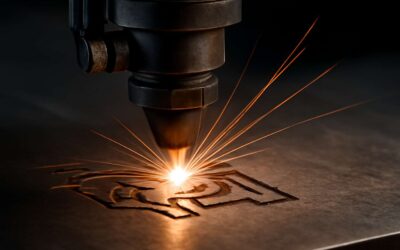
In the dim glow of innovation, choosing the right laser engraver pcb machine becomes an act of artistry—a delicate dance between precision and power. Among the contenders, CO2 laser engravers stand as stalwart artisans, wielding their beams with finesse to carve intricate pathways into the very fabric of printed circuit boards. Their ability to produce fine, detailed engravings makes them a favorite for manufacturers seeking both speed and sophistication.
What sets CO2 laser engravers apart is their versatility. They excel at working on various materials such as fiberglass, acrylic, and even thin copper layers, making them indispensable for modern PCB fabrication. For those seeking optimal performance, understanding the type of laser engraver pcb best suited to your project is paramount.
- High-powered CO2 lasers for rapid prototyping
- Mid-range models balancing speed with detail
- Desktop units perfect for small-scale production or hobbyist endeavors
Ultimately, selecting the ideal laser engraver pcb is a journey—one that combines technological prowess with creative vision, forging pathways into the future of electronic craftsmanship. Each beam, each cut, etches not just a circuit but the very essence of ingenuity itself.
Fiber Laser Engravers
When it comes to laser engraver pcb fabrication, fiber laser engravers are often the unsung heroes—less flashy than their CO2 cousins but incredibly efficient in their own right. These marvels of modern machinery use a concentrated beam of light to etch, mark, and cut with pinpoint accuracy, making them ideal for detailed PCB work. Their ability to handle metals like copper with finesse transforms the way circuit boards are manufactured, especially when precision is non-negotiable.
For those wondering about the best fit for their project, fiber laser engravers for pcb fabrication offer a distinct advantage: they don’t require consumables like gases or mirrors, reducing long-term operational costs. Plus, their high energy density allows for faster processing times—a blessing for rapid prototyping or high-volume production. Whether you’re crafting intricate circuit pathways or marking components, these laser engraver pcb machines deliver consistent, high-quality results without breaking the bank.
- Speed and efficiency in metal engraving
- Exceptional precision for complex circuitry
- Minimal maintenance and operational costs
In the realm of laser engraver pcb manufacturing, fiber laser technology is a game-changer—combining the allure of innovation with the practicality of industrial-grade performance. It’s a tool that elevates the craft of circuit board creation and ensures that every etched pathway is as perfect as the design behind it.
UV Laser Engravers
When considering the spectrum of laser engraver pcb options, UV laser engravers stand out as a sophisticated choice for intricate circuit work. Unlike their more common counterparts, UV laser engravers emit a shorter wavelength of light, allowing for remarkably precise etching on delicate substrates. This level of finesse is particularly advantageous in the realm of high-density PCB fabrication, where every micron counts.
These devices excel in creating complex circuitry with minimal thermal impact, preserving the integrity of sensitive components. Their ability to produce ultra-fine lines and intricate patterns makes them indispensable for advanced electronic applications. For those seeking exceptional detail without compromising speed, UV laser engravers for pcb manufacturing present an elegant solution—merging technological innovation with meticulous craftsmanship.
- Superior resolution for detailed circuit pathways
- Minimal heat-affected zones, protecting delicate materials
- Enhanced versatility for various PCB substrates
In the competitive landscape of PCB production, integrating a UV laser engraver pcb system can elevate quality standards while streamlining complex design execution. It’s a tool that embodies both precision and finesse, essential for pushing the boundaries of modern electronic manufacturing in South Africa and beyond.
Choosing the Right Laser for PCB Applications
Choosing the right laser engraver pcb system hinges on understanding the specific demands of your project. Different types of laser engravers offer distinct advantages tailored to PCB fabrication. For instance, UV laser engravers excel at producing ultra-fine circuit pathways, making them ideal for high-density PCB manufacturing where precision is paramount. Their capability to etch delicate substrates with minimal thermal impact ensures the integrity of intricate designs.
Meanwhile, fiber laser engravers are known for their efficiency and durability, often used for marking and engraving metal components in PCB assemblies. CO2 laser engravers, on the other hand, are versatile and cost-effective for general PCB etching and surface marking tasks. Each type of laser engraver pcb has its niche, and selecting the appropriate one depends on factors like resolution requirements, substrate compatibility, and production volume. The decision often boils down to balancing speed, detail, and material compatibility, ensuring the final product meets modern electronic standards in South Africa and beyond.
Step-by-Step Process of Laser Engraving PCBs
Design Preparation and File Conversion
Preparing your design for laser engraver PCB work is a crucial step that transforms a simple concept into a precise masterpiece. This process begins with creating a detailed digital layout, often crafted in specialized CAD software that allows for meticulous control over every trace and pad. Once the design is finalized, it’s essential to convert it into a compatible file format—typically a vector-based format like SVG or DXF—that the laser engraver PCB can interpret flawlessly. This conversion ensures that the intricate details of your design are preserved, maintaining the high precision that laser technology is renowned for.
Next, a thorough review of the file ensures that all elements are correctly scaled and positioned. It’s advisable to simulate the engraving process within the software, which helps anticipate potential issues before the laser interacts with the material. During this phase, adjusting parameters such as laser power, speed, and focus can significantly impact the quality of the final result. When everything aligns perfectly, the design file is ready to feed into the laser engraver PCB, setting the stage for a seamless and accurate engraving process that elevates your project to new heights of craftsmanship!
Material Selection and Preparation
When embarking on the journey of creating a laser engraver PCB, the selection and preparation of the right material can transform a mere concept into a masterpiece of technological artistry. The allure of a flawless circuit begins with choosing substrates that balance conductivity with durability, such as copper-clad boards or specialized composite materials tailored for laser precision. Each material’s unique characteristics influence not only the quality of the engraving but also the longevity of the finished product.
Preparing these materials involves meticulous cleaning and surface treatment to ensure optimal laser interaction. A pristine surface guarantees that the laser’s energy is efficiently absorbed, producing crisp, clean lines that are vital for high-quality PCB fabrication. In some cases, applying a thin layer of protective coating can enhance contrast and prevent unintended burn marks, ensuring that every detail remains sharp and accurate.
For those seeking an impeccable finish, consider the following points when selecting your material:
- Material compatibility with laser engraving technology
- Thermal stability under laser exposure
- Ease of cleaning and preparation
- Electrical properties suitable for PCB applications
In the realm of laser engraver PCB production, each choice echoes in the final product’s precision and performance, underscoring the importance of deliberate material selection and preparation. When these elements align harmoniously, the potential for innovation becomes boundless—where artistry meets engineering in a dance as old as time itself.
Laser Parameter Setting
Setting the laser parameters for engraver PCB production is where precision truly takes flight. It’s a delicate dance between laser power, speed, and focus—each one critical in shaping the final masterpiece. When fine-tuning these settings, consider the specific material properties; a copper-clad board demands different energy levels than a composite substrate. Small adjustments can mean the difference between a crisp, detailed circuit and a smudged, unusable design.
To streamline this process, many experts rely on a systematic approach, often employing a simple
- trial engrave
- measurement of line width
- adjustment of laser intensity
cycle. This iterative method ensures the laser engraver pcb produces consistent, high-quality results. Mastery of these parameters transforms raw material into a precise, durable circuit—an intersection of art and engineering that celebrates the allure of innovation.
Engraving and Etching
Embarking on the journey of laser engraver PCB production is akin to navigating a labyrinth of precision and artistry. The process demands meticulous orchestration, where each step builds upon the last to forge a circuit that is both resilient and intricate. Once the design is prepared and the material selected, the actual engraving and etching become a dance of light and shadow—transforming digital dreams into tangible reality.
In this phase, the laser engraver PCB operates with a delicate balance. It begins with the controlled emission of laser pulses, carefully calibrated to etch away unwanted material while preserving the fine lines that define your circuit. A systematic approach often guides this process, involving iterative adjustments to laser intensity, speed, and focus—each tweak honing the precision of the final product.
To enhance efficiency, many artisans employ a straightforward yet effective method: conducting test engravings to measure line widths and refine laser parameters. This cyclical process—engraving, measuring, adjusting—ensures that each circuit maintains impeccable detail, from micro traces to complex multilayer configurations. Ultimately, mastery over these steps transforms raw PCB material into a durable, high-performance component—an intersection where engineering excellence meets artistic finesse.
Post-Processing and Quality Inspection
Post-processing and quality inspection are the final, vital acts in the symphony of laser engraver PCB production. Once the initial etching and engraving are complete, meticulous scrutiny ensures each circuit meets the highest standards of precision and durability. Visual inspection under magnification reveals micro flaws—tiny imperfections that could jeopardize performance. This stage is crucial for identifying any inconsistencies that may have arisen during the laser engraving process.
To guarantee flawless results, many artisans employ a combination of manual inspection and advanced testing methods. For example, electrical testing verifies that all traces are correctly connected and free of shorts or open circuits. This step is often followed by a thorough cleaning process, removing any residual debris or unetched material that might interfere with the PCB’s operation.
For enhanced accuracy, an ordered checklist can streamline the inspection process:
- Visual examination for surface defects or irregularities.
- Electrical continuity testing to confirm circuit integrity.
- Dimensional measurement to ensure adherence to design specifications.
- Final cleaning and surface treatment to prepare the PCB for assembly.
Mastering these post-processing steps transforms a raw, laser-engraved PCB into a resilient masterpiece of engineering craftsmanship. The magic of laser engraver pcb lies not just in the engraving itself, but in the precision and care taken during these critical finishing touches—turning digital visions into tangible, functioning marvels.
Common Materials Used in Laser PCB Engraving
FR-4 and Other Substrates
When exploring the realm of laser engraver PCB, understanding the materials that withstand the precision and intensity of laser technology is crucial. Among these, FR-4 remains the gold standard—a composite of woven fiberglass cloth with an epoxy resin binder that offers remarkable durability and stability. Its resilience under laser engraving makes it a preferred choice for intricate circuit patterns, ensuring longevity and performance. But other substrates also find their place in the laser PCB landscape.
Materials like polyimide and acrylic are gaining popularity due to their flexibility and ease of engraving. Polyimide, with its high heat resistance, supports complex designs without warping, while acrylic provides a clean, glossy finish that enhances visual appeal. For specialized applications, ceramic-based substrates are also employed, offering exceptional heat dissipation. Whether working with FR-4 or alternative substrates, selecting the right material ensures the laser engraver pcb process achieves optimal precision and quality. Incorporating these diverse materials into your workflow can elevate the craftsmanship and functionality of your designs, capturing the true artistry behind laser engraving technology.
Copper Sheets and Clad Materials
When it comes to laser engraver PCB manufacturing, copper sheets and clad materials are at the heart of the process. Copper’s excellent electrical conductivity makes it an ideal choice for creating precise circuit pathways, especially when combined with laser technology that can meticulously engrave intricate designs. With laser engraver PCB projects, the quality of the copper or clad substrate directly impacts the performance and durability of the final product.
Commonly used copper sheets include rolled copper, etched copper, and clad laminates, each offering unique advantages. For complex, high-density circuits, copper clad laminates with a thin layer of copper bonded to a non-conductive substrate are preferred. These materials support fine detailing and are compatible with various laser parameters for clean, sharp engravings. Additionally, some manufacturers opt for pure copper sheets to maximize thermal and electrical properties, especially in high-power applications.
To ensure optimal results, selecting the right copper or clad material involves considering factors like thickness, surface finish, and compatibility with the laser engraver PCB process. Whether working with standard copper sheets or specialized clad substrates, understanding the nuances of these materials can elevate the precision and craftsmanship of your laser-etched circuits, delivering superior quality and reliability in your designs.
Photoresist Films
When it comes to laser engraver PCB manufacturing, the choice of photoresist films plays a pivotal role in achieving high-quality results. Unlike traditional methods, laser engraving allows for precise control over the exposure process, making the type of photoresist film crucial. These materials need to withstand laser heat while providing sharp, clear patterns. Commonly used photoresist films include dry film photoresists, liquid photoresists, and bi-layer systems, each suited to different application needs.
For intricate, fine-line circuits, manufacturers often prefer dry film photoresist due to its excellent adhesion and smooth surface finish. Liquid photoresists, on the other hand, are favored for their flexibility and ease of application on complex geometries. The choice of photoresist film directly influences the clarity of the laser-etched pattern and the durability of the PCB. Selecting the right material ensures that the laser engraver PCB process yields precise, consistent, and high-performance circuit boards, meeting the stringent demands of modern electronic devices.
Alternative Materials
When navigating the intriguing realm of laser engraver PCB manufacturing, it’s essential to appreciate the palette of materials that make this precision art possible. While copper sheets and clad materials are the backbone, alternative materials are gaining momentum for their unique advantages. Among these, polymer-based substrates and specialized ceramics stand out, especially when high-temperature resistance and durability are paramount. These materials can withstand the intense heat generated during laser engraving, ensuring crisp, detailed circuit patterns without warping or degradation.
For those seeking versatility, laser-compatible masking tapes and etch-resistant coatings provide an extra layer of finesse. They serve as protective barriers, enabling intricate designs to be executed with surgical precision. A noteworthy trend is the use of photoresist films—dry, liquid, or bi-layer systems—each offering tailored solutions for specific project needs. Selecting the appropriate material not only optimizes the laser engraver PCB process but also ensures the final product boasts high reliability and performance, vital in today’s competitive electronic landscape.
Design Considerations for Laser Engraved PCBs
Circuit Traces and Line Width
When designing a circuit for a laser engraver pcb, precision becomes the currency of success. The intricate dance between trace width and spacing demands meticulous attention, as even the slightest deviation can ripple through the entire functionality of the final product. Line width, in particular, is pivotal—too narrow, and the risk of breakage or incomplete etching looms; too broad, and you sacrifice the compactness vital for modern electronic devices.
To optimize your laser engraver pcb design, consider the following essential factors: the type of substrate, the laser’s power density, and the desired electrical performance. A nuanced understanding of these parameters ensures that traces are not only visually sharp but also electrically resilient. When preparing your files, employing vector graphics with precise line width specifications safeguards against inconsistencies during the engraving process.
Additionally, the choice of line width should balance production feasibility with performance demands. For instance, high-frequency circuits require narrower traces to minimize parasitic inductance, yet wider traces may be necessary for current-carrying capabilities. Engaging with these design considerations paves the way for a laser engraver pcb that exemplifies both innovation and reliability.
Drill Hole Precision
In the realm of laser engraver pcb design, the pursuit of flawless drill hole precision is akin to chasing a whisper in the wind—delicate yet vital. Every tiny hole must align perfectly, serving as the gateway for pins and connectors that breathe life into your circuit. Achieving this level of accuracy demands meticulous calibration of laser parameters, ensuring each hole is clean, round, and consistent. This is no ordinary task; it’s an intricate dance between machine capability and material response.
When working with laser engraver pcb, consider the substrate’s nature—whether it’s a sturdy FR-4 or a more flexible composite—as it influences how the laser interacts with the material. For optimal results, employ
- precise vector files
- adjusted laser power
- appropriate dwell time
to hone in on the perfect drill hole. The key is balancing speed with accuracy, avoiding overshoot that could distort hole dimensions or undercut that leaves gaps in electrical connectivity. Such precision not only enhances the aesthetic finesse of the finished product but also fortifies the electrical resilience of your circuit.
In the delicate world of laser engraver pcb, every detail counts—especially the drill holes that serve as the backbone of your design. Mastery over these parameters transforms a simple pattern into a symphony of technological artistry, where each hole sings in harmony with the entire circuit’s function and form.
Component Placement and Alignment
When it comes to laser engraver pcb design, component placement and alignment are more than mere technicalities—they are the very essence of functional artistry. Precision in positioning parts ensures that each pathway and connection aligns seamlessly, transforming a chaotic scatter of components into a symphony of electrical harmony. The challenge lies in maintaining this meticulous alignment throughout the manufacturing process, where even the slightest deviation can ripple into costly errors or compromised performance.
In the realm of laser engraver pcb, thoughtful consideration of component placement involves assessing the spatial relationship between elements—ensuring sufficient clearance, optimizing heat dissipation, and facilitating ease of assembly. Alignment, on the other hand, demands an unwavering focus on accuracy, often achieved through specialized fixture setups or calibration routines that fine-tune the laser’s focus and positioning. Such attention to detail is vital, as it directly influences the reliability of drilled holes and the integrity of delicate traces.
To streamline this process, many designers adopt a strategic approach, such as utilizing
- high-precision vector files
- adjusted laser parameters
- rigid fixturing systems
that safeguard component integrity. This ensures every element, from tiny surface-mount devices to complex connectors, is perfectly aligned—an essential factor when working with advanced laser engraver pcb systems. Ultimately, mastering component placement and alignment elevates the craft from mere manufacturing to a form of technological artistry—where each detail sings in flawless harmony within the circuit’s grand design.
Design Software Compatibility
When it comes to laser engraver pcb design, software compatibility isn’t just a technical checkbox—it’s the secret sauce that ensures your circuit dreams become reality. A mismatch between your design software and the laser engraver system can turn a straightforward project into a frustrating game of digital hide-and-seek. To avoid this, choose software that seamlessly integrates with your laser engraver pcb workflow, supporting popular formats like Gerber, DXF, or proprietary files optimized for precision. This ensures that every trace, via, and component footprint translates perfectly from screen to substrate.
Furthermore, compatibility extends beyond file formats. Opt for design software that offers robust calibration routines and real-time preview features, allowing you to fine-tune laser parameters before the actual engraving process. This not only boosts accuracy but also reduces material waste—an essential consideration in resource-conscious environments like South Africa. Whether you’re working with fiber laser engravers or UV laser systems, ensuring your software aligns with your hardware capabilities can make all the difference, transforming your laser engraver pcb projects from guesswork into a symphony of precision engineering.
Challenges and Limitations of Laser Engraving PCBs
Material Restrictions
Laser engraver PCB technology has revolutionized how we approach circuit board fabrication, but it’s not without its hurdles. Material restrictions pose a significant challenge, especially when working with diverse substrates. Not all materials are compatible with laser engraving, and selecting the wrong type can lead to poor engraving quality or damage to the PCB. For example, while FR-4 is the standard, other materials like flexible polyimide films or ceramic substrates may not respond well to certain laser settings.
Limitations in material selection can also restrict design flexibility. Some materials cannot withstand the heat generated during laser engraving, resulting in uneven traces or delamination. This means manufacturers must carefully balance laser parameters with material properties. Additionally, the thickness of copper sheets and clad materials impacts the effectiveness of the laser engraver PCB process. Thicker copper layers require more power and precision, which can complicate production. As a result, understanding these material restrictions is crucial for achieving high-quality results in laser PCB manufacturing.
Fire Risk and Safety Measures
While the marvel of laser engraver PCB technology continues to transform circuit board manufacturing, it harbors inherent challenges that demand respect and understanding. Among these, fire risk stands prominently as a formidable obstacle. The intense heat generated during laser engraving can ignite flammable materials or produce hazardous fumes, especially when working with certain substrates. Ensuring safety measures are in place becomes not just prudent but essential to prevent accidents and equipment damage.
Safety protocols often include the following measures:
- Proper ventilation systems to disperse fumes and reduce fire hazards
- Use of fire-resistant enclosures and fire extinguishers nearby
- Regular maintenance and calibration of the laser to prevent unintended sparks or overheating
In addition to these precautions, operators must vigilantly monitor laser parameters such as power, speed, and focus, as improper settings can escalate fire risks. The delicate balance between achieving high-quality circuit traces and maintaining safety is a constant dance—one that requires a keen eye and thorough preparation. When harnessed carefully, a laser engraver PCB becomes a tool of extraordinary precision and efficiency, but neglecting safety can turn this technological marvel into a perilous endeavor. Embracing these safety measures ensures that the process remains not only effective but also secure, safeguarding both personnel and equipment in this enchanted realm of PCB manufacturing.
Size Limitations
When it comes to laser engraver pcb technology, size limitations often present a significant challenge. Despite the remarkable precision and efficiency this method offers, working within confined dimensions can restrict the complexity of designs and the scale of projects. Small-scale or intricate circuits may be perfectly suited, but larger or more expansive boards can push the boundaries of what a laser engraver pcb can achieve effectively.
One of the primary constraints lies in the working bed size of the engraver, which can vary greatly depending on the model. For instance, compact desktop units are ideal for prototypes or small batches but may struggle with larger PCBs. Conversely, industrial-grade systems can accommodate bigger boards, yet they come with higher costs and increased setup complexity. This size limitation often necessitates dividing large designs into smaller sections, then aligning and assembling them post-engraving—a process that demands patience and meticulous attention to detail.
- Designs exceeding the engraver’s bed dimensions require segmentation, increasing the risk of misalignment.
- Material handling becomes more cumbersome, especially when working with thick substrates or multiple layers.
- Ensuring uniform engraving across larger areas demands precise calibration, further complicating the process.
For those venturing into extensive PCB projects, understanding these size limitations of laser engraver pcb systems is crucial. While advancements continue to push the envelope, recognizing the boundaries helps in planning efficient workflows and avoiding costly setbacks. In the end, embracing these challenges transforms the process into an art form—balancing technical constraints with craftsmanship, ensuring each circuit bears the hallmark of precision and care.
Cost of Equipment
The cost of equipment for laser engraver pcb projects can be a significant hurdle, especially for small businesses or hobbyists. High-end industrial systems can run into hundreds of thousands of rand, making the initial investment daunting. Even compact desktop units, while more affordable, still require a substantial outlay—often necessary to ensure quality and precision in intricate PCB designs.
Beyond the purchase price, maintenance and calibration add to the overall expense. Precise calibration is essential for achieving uniform engraving, yet it demands ongoing investment in skilled labor and spare parts. For those exploring laser engraver pcb technology, understanding these financial commitments is crucial to avoid unexpected setbacks that could derail a project’s success.
Additionally, the complexity of the equipment can lead to a steep learning curve. Mastering the nuances of laser parameters, material handling, and safety protocols can require significant time and resources. For large-scale projects, this translates into higher operational costs and extended timelines, amplifying the importance of weighing the initial investment against long-term productivity gains.
- High initial costs for industrial-grade laser engraver pcb systems
- Ongoing expenses for maintenance and calibration
- Steep learning curve impacting operational costs
As laser engraver pcb technology advances, more affordable options are emerging, but the core challenge remains: balancing budget constraints with the demand for precision and efficiency. This financial dimension often determines whether a project is feasible or if alternative manufacturing methods should be considered.
Future Trends in Laser PCB Engraving Technology
Automation and AI Integration
As technology continues to evolve at an unprecedented pace, the future of laser engraver PCB manufacturing is poised for remarkable transformation. Automation and AI integration are at the forefront, promising to streamline processes, enhance precision, and reduce human error—an essential leap forward for the electronics industry. Imagine a scenario where laser engraver PCB systems can self-optimize their parameters based on real-time feedback, ensuring consistent quality across large production runs. This level of sophistication not only accelerates throughput but also elevates safety standards, minimizing risks associated with manual intervention.
Furthermore, the integration of artificial intelligence enables predictive maintenance, reducing downtime and prolonging equipment lifespan—a vital advantage in high-volume manufacturing environments. As these systems become increasingly intelligent, they will support complex designs with intricate circuit traces and ultra-fine line widths, pushing the boundaries of what can be achieved with laser engraver PCB technology. The convergence of automation and AI heralds a new era where precision, efficiency, and flexibility are seamlessly aligned to meet the demands of tomorrow’s innovative electronics landscape.
- Enhanced design flexibility through adaptive laser settings
- Smarter material handling and waste reduction
- Real-time quality assurance and defect detection
Enhanced Material Compatibility
The future of laser engraver PCB technology is unfolding in a landscape marked by unprecedented material versatility. As industries demand increasingly complex and miniaturized circuits, the ability to work with a broader spectrum of substrates becomes critical. Enhanced material compatibility is no longer a luxury but a necessity, enabling manufacturers to push the boundaries of innovation. This evolution is driven by sophisticated laser systems capable of adjusting parameters in real-time, ensuring optimal engraving on diverse materials such as flexible films, composite laminates, and advanced ceramics.
Such adaptability not only expands design possibilities but also fosters sustainable practices by reducing waste and optimizing material usage. The integration of smarter material handling systems means that the laser engraver pcb can seamlessly switch between substrates, minimizing downtime and elevating production efficiency. As these advancements become mainstream, they empower engineers to explore ultra-fine circuit traces and intricate geometries that were previously unattainable, heralding a new epoch of precision and creativity in PCB manufacturing.
Miniaturization and Complex Designs
As the world of electronics marches toward ever-smaller, more intricate circuits, laser engraver pcb technology is stepping up to meet the challenge. Miniaturization isn’t just a trend; it’s the new standard, demanding precision tools capable of crafting ultra-fine traces and complex geometries with ease. Gone are the days when bulky, manual methods dictated circuit design—today’s laser systems can produce detailed patterns that would make even the most meticulous engineer smile.
Future trends indicate that laser engraver pcb machines will continue to push the envelope, integrating advanced features like multi-material compatibility and real-time parameter adjustment. This means manufacturers can now work seamlessly with substrates such as flexible films, composite laminates, and even advanced ceramics—materials that were once considered off-limits. The result? A surge in innovative design possibilities, from multi-layered PCBs to intricate, miniaturized components that fit into tiny spaces without sacrificing performance.
Additionally, the rise of automation and AI-driven controls means that laser engraver pcb systems will soon operate with minimal human intervention, optimizing engraving paths and reducing errors. As a result, engineers can focus more on creative circuit layouts while the machines handle the precision work. This fusion of miniaturization and complex design capabilities heralds a new era of PCB manufacturing—more efficient, more precise, and more adaptable than ever before.
Environmental Impact and Sustainability
As laser engraver pcb technology advances, the focus on environmental impact and sustainability becomes increasingly vital. Manufacturers are now exploring eco-friendly laser systems that reduce energy consumption and minimize hazardous emissions, aligning with global efforts to green electronics production. Innovations such as optimized laser pathways and power-efficient modules not only lower operational costs but also diminish carbon footprints.
Future trends point toward the integration of sustainable materials and recycling-friendly processes, ensuring that PCB manufacturing remains environmentally conscious. For example, the use of biodegradable substrates and recyclable copper clads is gaining traction, allowing the industry to reduce waste and promote circular economy principles.
Incorporating these sustainable practices into laser engraver pcb systems helps foster a greener industry. As a result, companies can meet stricter environmental standards while maintaining high-precision, complex designs that laser systems excel at. Advancements in laser technology continue to push the boundaries, making eco-friendly PCB manufacturing not just a possibility but a standard.
0 Comments